High-End Performance Packaging Market Outlook: AI Chip Integration, Advanced Packaging Technologies, Manufacturing Yield, and Supply Chain Resilience
High-End Performance Packaging Market: 6 Decisions Companies Should Make to Strengthen AI Chip Integration, Improve Yield, and Secure Supply Chains
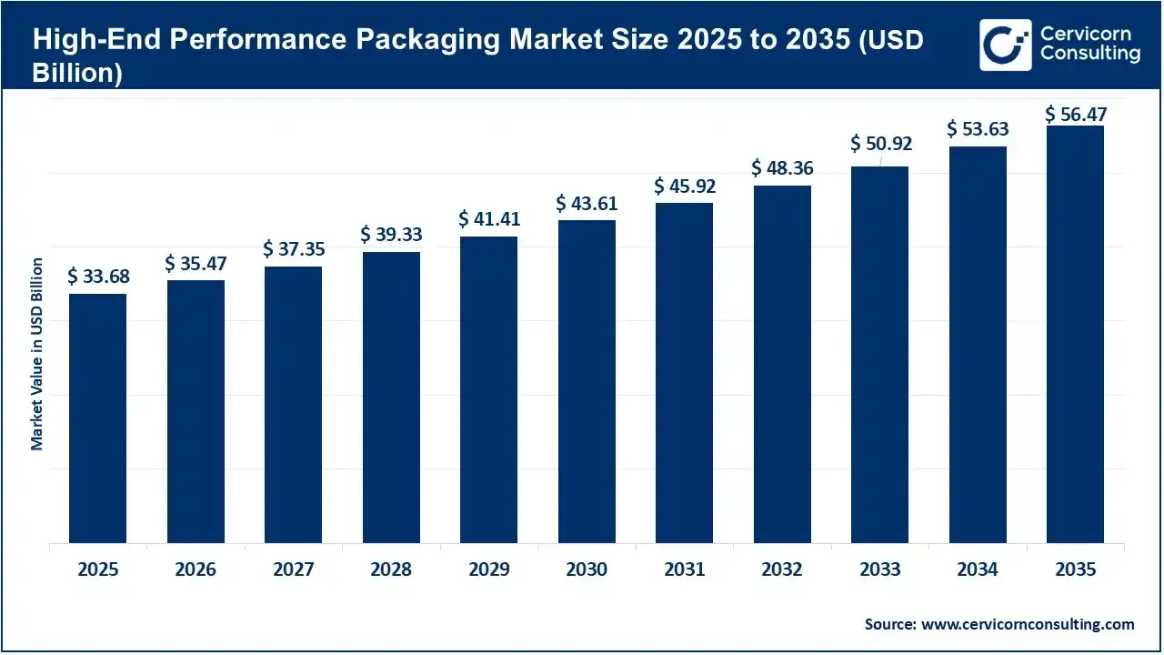
The global high-end performance packaging market was valued at USD 33.68 billion in 2025 and is projected to reach USD 56.47 billion by 2035, growing at a compound annual growth rate (CAGR) of 5.3% from 2026 to 2035, according to Cervicorn Consulting’s market estimates. Demand is being shaped by AI accelerators, high-bandwidth memory (HBM), chiplet integration, 2.5D and 3D packaging, and the need to deliver higher computing performance within increasingly constrained power and thermal envelopes.
For semiconductor manufacturers, outsourced semiconductor assembly and test (OSAT) providers, substrate manufacturers, materials suppliers, and equipment companies, the strategic question is not simply which packaging technology will grow fastest. It is which architectures can deliver commercially viable performance, reliable manufacturing yields, predictable delivery schedules, and sufficient capacity as customer requirements become more demanding.
Advanced packaging decisions now influence product roadmaps, capital expenditure, supplier selection, and time to market. Companies that align packaging architecture with application requirements and manufacturing economics will be better positioned to capture demand while limiting technical and operational risks.
1. Should Companies Prioritize 2.5D Packaging, 3D Integration, or Chiplet-Based Architectures?
The first decision is determining how much integration a product genuinely requires. As conventional transistor scaling becomes more challenging and expensive, manufacturers are increasingly combining multiple dies, logic components, and memory within a single package. However, not every application requires the highest level of integration.
The decision should be based on performance requirements, interconnect density, thermal constraints, manufacturing yield, and total package cost rather than technology novelty alone.
- 2.5D packaging: Suitable for applications requiring high-bandwidth communication between logic and memory dies, particularly AI accelerators and high-performance computing (HPC) processors.
- 3D packaging: Relevant when vertical integration, shorter interconnects, and greater computing density justify more demanding thermal management and manufacturing processes.
- Chiplet integration: Enables manufacturers to combine different functional dies within a package, potentially improving design flexibility and allowing different components to use different process technologies.
- Flip-chip packaging: Remains relevant for established high-performance processors and networking devices that require dense electrical connections and effective thermal pathways.
- System-in-Package (SiP): Can support compact integration of multiple functional components where board space, functionality, and system-level integration are important.
Cervicorn Consulting’s market analysis identifies flip-chip packaging as the leading packaging type in 2025, with an estimated 28% revenue share. Meanwhile, 3D packaging is positioned for faster expansion as demand for higher integration density increases.
Business implication: Companies should evaluate packaging architectures against workload requirements, die size, memory bandwidth, expected production volume, and cost per usable package. A modular chiplet design may offer greater flexibility, while a more integrated architecture may be justified when performance gains outweigh additional design and manufacturing complexity.
Get a Free Sample: https://www.cervicornconsulting.com/sample/3069
2. How Should Companies Prepare for the Shift Toward Hybrid Bonding and Advanced Interconnects?
As processors integrate more dies and memory components, conventional interconnect approaches can become limiting factors. Hybrid bonding, through-silicon vias (TSVs), silicon interposers, and other high-density interconnect technologies are therefore becoming important considerations in next-generation packaging roadmaps.
Cervicorn Consulting estimates that TSV technology accounted for approximately 27% of the high-end performance packaging market in 2025. Chiplet integration represented another important technology segment, reflecting the growing need to connect multiple functional components within advanced semiconductor systems.
Companies should assess these technologies according to their current capabilities and target applications.
- TSVs: Evaluate their suitability for vertical electrical connections and stacked-die architectures, particularly where memory bandwidth and integration density are critical.
- Hybrid bonding: Assess whether finer interconnect pitches and improved die-to-die connectivity justify the additional process development, equipment, and inspection requirements.
- Chiplet integration: Establish compatible interface specifications, design rules, and testing procedures before committing to multi-vendor architectures.
- Wafer-level and fan-out packaging: Determine whether these approaches can satisfy package size, electrical performance, and production requirements at competitive cost.
Hybrid bonding can create opportunities for higher-density integration, but implementation depends on process maturity, surface preparation, alignment accuracy, defect control, and the ability to maintain acceptable yields at production scale.
Business implication: Packaging technology investments should follow product roadmaps and customer qualification schedules. Companies should identify which interconnect capabilities they need to develop internally, which can be obtained through external partners, and which technologies require pilot production before a major capital commitment.
3. Can the Supply Chain Support Higher Volumes Without Increasing Cost and Delivery Risk?
High-end performance packaging depends on a coordinated ecosystem of foundries, OSAT providers, substrate manufacturers, materials suppliers, equipment vendors, and semiconductor designers. A package can be technically feasible but commercially difficult to scale if a critical interposer, substrate, bonding process, or testing capability is unavailable.
Capacity planning has consequently become a strategic priority. Companies must consider not only current production availability but also future customer demand, qualification lead times, geographic concentration, and the cost of reserving additional capacity.
Key actions include:
- Map critical dependencies: Identify single-source materials, specialized substrates, advanced bonding equipment, and outsourced testing capabilities that could constrain production.
- Qualify alternative suppliers: Establish technically acceptable alternatives where feasible, while accounting for the time and cost required for customer requalification.
- Align capacity with demand visibility: Use customer forecasts, design-win pipelines, production commitments, and scenario analysis to determine when additional capacity is justified.
- Evaluate geographic exposure: Assess the implications of concentrated manufacturing networks, export restrictions, logistics disruptions, and regional investment incentives.
- Coordinate development earlier: Bring packaging partners into product design discussions before specifications become difficult or expensive to change.
Asia-Pacific remains central to the industry’s manufacturing and assembly ecosystem. Cervicorn Consulting estimates that the region accounted for approximately 46% of the global market in 2025, supported by its established semiconductor production and packaging base.
At the same time, investments in domestic semiconductor manufacturing and advanced packaging capacity are creating opportunities in North America and other emerging production hubs.
Business implication: Procurement and operations leaders should measure supply-chain resilience using more than supplier count. Qualification readiness, available capacity, lead-time variability, recovery options, and the commercial cost of switching suppliers are equally important.
4. Which Packaging Materials Offer the Best Balance of Performance, Availability, and Cost?
Packaging materials influence electrical performance, thermal management, mechanical stability, reliability, and manufacturing yield. As package dimensions shrink and integration density rises, substrate and material selection becomes increasingly important to overall product performance.
Cervicorn Consulting estimates that organic substrates accounted for approximately 34% of market revenue in 2025, reflecting their established role across advanced semiconductor packaging applications.
However, materials decisions should not be based on market share alone. Different package architectures place different demands on substrates, interposers, underfills, encapsulants, and die-attach materials.
- Organic substrates: Evaluate for established manufacturing processes, versatility, cost, and compatibility with the required package design.
- Silicon interposers: Consider where dense interconnects between logic and memory components are required.
- Glass substrates: Assess their potential dimensional stability and high-density interconnect capabilities, while examining production maturity, reliability, and supply availability.
- Mold compounds and encapsulants: Compare their protection, mechanical properties, thermal characteristics, and compatibility with package geometry.
- Underfill and die-attach materials: Evaluate their contribution to mechanical reliability, interconnect protection, and thermal or electrical requirements.
Material qualification should include thermal cycling, moisture resistance, warpage, mechanical stress, electrical performance, and compatibility with downstream assembly processes. For advanced packages, a material that performs well in isolation may still create difficulties when combined with other components or manufacturing steps.
Business implication: Materials suppliers should identify the specific performance constraints faced by their target package architectures. Semiconductor manufacturers should evaluate materials through package-level testing and total manufacturing economics rather than relying exclusively on unit price or individual material specifications.
5. How Can Companies Control Thermal Performance, Power Delivery, and Manufacturing Yield?
AI accelerators and high-performance computing packages increasingly combine powerful logic dies with high-bandwidth memory and dense electrical interconnects. These designs can concentrate substantial heat within limited package volumes, creating challenges for cooling, power delivery, signal integrity, and long-term reliability.
Thermal and yield issues can undermine the commercial value of an otherwise high-performing package. A design that meets performance targets but requires expensive cooling, extensive rework, or low-yield production may struggle to achieve acceptable economics.
Companies should integrate the following considerations into package development:
- Thermal simulation: Model heat distribution across logic dies, memory stacks, interposers, substrates, and package interfaces before finalizing the architecture.
- Power-delivery design: Assess voltage delivery, electrical resistance, current density, and power-distribution requirements under realistic workloads.
- Warpage and mechanical reliability: Evaluate material expansion, die stacking, package deformation, and solder-joint reliability across operating conditions.
- Defect inspection: Strengthen inspection and test coverage for bonding interfaces, interconnects, and multi-die assemblies.
- Yield improvement: Track yield at individual process stages and across the completed package to identify the operations responsible for the largest losses.
- Design-for-manufacturing collaboration: Involve packaging engineers, chip designers, materials specialists, and test teams early enough to prevent avoidable redesigns.
The financial impact should be assessed using cost per good package rather than nominal assembly cost alone. Scrap, rework, inspection, test time, warranty exposure, and delayed customer qualification can materially change the economics of competing technologies.
Business implication: Engineering and manufacturing teams should establish shared targets for thermal performance, package reliability, production yield, and cost per usable unit. These metrics allow companies to compare alternative architectures using both technical and commercial criteria.
6. Where Should Companies Focus Their Next Investments: AI, Data Centers, Automotive, or Networking?
High-end performance packaging serves multiple applications, but each market has distinct performance requirements, qualification cycles, and demand patterns. Companies should choose investment priorities based on their existing capabilities, customer access, and expected returns rather than treating every growing application as an equally attractive opportunity.
Cervicorn Consulting estimates that artificial intelligence and high-performance computing accounted for approximately 32% of market revenue in 2025, making it the largest application segment in its market analysis.
The main application opportunities differ in several ways:
- AI and high-performance computing: Demand high-bandwidth memory integration, dense interconnects, advanced thermal management, and increasingly complex multi-die architectures.
- Data centers and cloud computing: Create opportunities linked to accelerators, networking processors, memory integration, and the need for higher computing throughput and energy efficiency.
- Telecommunications and networking: Require high-speed signal transmission, dependable performance, and packaging solutions suited to advanced networking hardware.
- Automotive electronics: Emphasize reliability, temperature tolerance, lifecycle support, and qualification requirements for safety- and mission-critical applications.
- Consumer electronics: Prioritize compact dimensions, power efficiency, cost control, and manufacturing at scale.
Companies should assess each opportunity against five factors: addressable customer demand, technical fit, qualification time, capital intensity, and achievable margin. A supplier with strong substrate or inspection capabilities may find a more attractive opportunity serving multiple packaging platforms than investing directly in a highly specialized assembly process. Conversely, a company with established AI accelerator relationships may justify deeper investment in high-density integration.
Regional investment decisions also require careful evaluation. Expanding capacity near customers can improve supply-chain responsiveness, but the business case depends on workforce availability, ecosystem maturity, equipment access, incentives, and long-term utilization.
Business implication: Prioritize investments where a company’s technical capabilities match identifiable customer requirements and where capacity can be utilized at commercially sustainable levels. Market growth alone does not guarantee attractive returns.
What Should Companies Do Next?
The high-end performance packaging market is evolving through the convergence of chiplets, 2.5D and 3D integration, high-bandwidth memory, advanced interconnects, and increasingly demanding AI workloads. However, the best commercial strategy will differ across semiconductor manufacturers, OSAT providers, materials companies, equipment suppliers, and investors.
A practical decision framework should connect technology selection with operational readiness and financial performance.
| Decision area | Key question | Recommended action |
|---|---|---|
| Packaging architecture | Which design meets performance and cost targets? | Compare 2.5D, 3D, chiplet, flip-chip, and SiP options against application requirements. |
| Technology roadmap | Which capabilities should be developed next? | Prioritize interconnect and bonding investments aligned with customer roadmaps. |
| Supply chain | Which dependencies could delay production? | Map critical suppliers, qualify alternatives, and assess capacity commitments. |
| Materials | Which materials deliver the required reliability and performance? | Validate options through package-level testing and total-cost analysis. |
| Manufacturing economics | Can the design achieve acceptable yield and cost per good unit? | Integrate thermal, power, inspection, and yield targets into development. |
| Market expansion | Which applications and regions fit existing capabilities? | Rank opportunities by customer access, qualification requirements, investment, and expected returns. |
Companies should review these decisions together rather than treating packaging technology, procurement, manufacturing, and market expansion as separate planning exercises. The strongest opportunities are likely to emerge where product performance, reliable supply, production economics, and customer demand reinforce one another.
To Get Detailed Overview, Contact Us: https://www.cervicornconsulting.com/contact-us
Read Report: Document AI Market Outlook: Workflow Automation, Data Accuracy, Enterprise Integration, and Scalable AI Adoption