


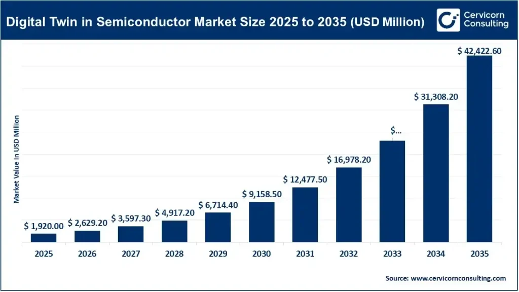
Digital Twin in Semiconductor Market Size
The global digital twin in semiconductor market size was valued at USD 1,920 million in 2025 and is projected to reach USD 42,422.6 million by 2035, representing a 36.2% CAGR.
Digital twin in semiconductor market growth factors
The digital twin in semiconductor market is gaining momentum as semiconductor manufacturers, foundries, integrated device manufacturers and chip-design companies seek to manage rising fabrication costs, increasingly complex process nodes, advanced packaging requirements and shorter product-development cycles. The technology creates virtual representations of semiconductor products, manufacturing equipment, production lines and entire fabs, allowing engineering teams to simulate processes, evaluate designs, monitor real-time performance and optimize operations before making changes to physical infrastructure.
Increasing adoption of AI, machine learning, IoT, edge computing, physics-based simulation and high-performance computing is strengthening the capabilities of semiconductor digital twins, while the expansion of AI chips, 3D ICs, chiplets and heterogeneous integration is increasing the need for system-level modeling. Government-backed semiconductor programs are also supporting the market. In the United States, the CHIPS for America program awarded $285 million to establish SMART USA, a Manufacturing USA institute focused specifically on digital twins for semiconductor design, manufacturing, advanced packaging, assembly and testing.
At the same time, companies such as Siemens, NVIDIA, Cadence, Dassault Systèmes and Synopsys are integrating digital twins with AI, simulation and electronic design automation, creating broader platforms for virtual semiconductor engineering and intelligent fabs.
Get a Free Sample: https://www.cervicornconsulting.com/sample/3039
What is digital twin in semiconductor market?
A digital twin in semiconductor is a virtual representation of a semiconductor product, manufacturing process, piece of equipment, production line or complete fabrication facility that is connected to data from its physical counterpart. The model can combine sensor data, engineering information, simulation models, process data and artificial intelligence to reproduce and analyze the behavior of the physical semiconductor environment.
In semiconductor manufacturing, digital twins can represent wafer-processing equipment, lithography processes, etching systems, deposition processes, cleanroom environments, HVAC systems, gas-flow networks and complete production lines. At the design level, they can model chips, packages, systems and their interaction with software.
Unlike a conventional simulation that may represent a process at a particular point in time, a digital twin can continuously incorporate real-world information and support monitoring, prediction and optimization. Synopsys describes semiconductor digital twins as virtual models that can be used to explore, analyze and optimize designs before they are finalized, while real-world data can subsequently be used to adjust or redesign systems.
This creates a connection between design, simulation, manufacturing and operations. For example, engineers can evaluate a proposed process change in a virtual fab before introducing it into the physical facility, potentially reducing disruption and allowing teams to identify problems earlier.
Why is digital twin important for the semiconductor industry?
Faster chip and process development
Advanced semiconductor development involves numerous iterations between design, simulation, fabrication and validation. Digital twins allow companies to perform more of these iterations virtually. Siemens notes that semiconductor digital twins can reduce iterations between design and production, enable virtual prototyping and support faster characterization and calibration of fab equipment.
Improved yield optimization
Yield is one of the most important performance indicators in semiconductor manufacturing. Small variations in temperature, pressure, contamination, equipment condition or process parameters can affect wafer quality. A digital twin can combine process information with historical and real-time data to identify relationships that may otherwise be difficult to detect.
Predictive maintenance
Semiconductor fabs contain highly sophisticated equipment that operates under tightly controlled conditions. Digital twins can help simulate equipment behavior and identify potential degradation before equipment failure occurs. This can support predictive maintenance and reduce unplanned downtime.
Lower development and manufacturing risk
Building semiconductor fabrication capacity requires substantial capital investment. Siemens has highlighted the high cost of fab construction and chip design as a major reason for increasing digitalization and the use of comprehensive digital twins.
Virtual testing allows manufacturers to assess alternative production strategies before modifying expensive physical infrastructure.
Energy and resource optimization
Fabs consume significant quantities of electricity, water, gases and other resources. Digital twins can model utilities and production processes to identify opportunities to optimize energy consumption, environmental conditions and equipment utilization.
Integration of AI and automation
The combination of AI with digital twins is becoming particularly important. AI can analyze large quantities of operational data, while the digital twin provides a physics-based or engineering context in which predictions can be tested. This combination is supporting the development of increasingly autonomous semiconductor manufacturing environments.
Leading companies in the digital twin in semiconductor market
The market involves companies from several adjacent technology categories, including industrial software, electronic design automation, simulation, GPU computing and engineering platforms. Because the digital twin in semiconductor market is not reported as a standardized standalone revenue segment by most suppliers, company-specific market shares are generally not publicly disclosed. Therefore, market-share figures should not be interpreted as audited company shares of the digital-twin market.
Siemens
Specialization: Industrial automation, EDA, digital manufacturing and industrial digital twins
Key Focus Areas: Semiconductor design, fab planning, manufacturing optimization, equipment modeling, predictive maintenance and smart manufacturing.
Notable Features: Siemens combines industrial software, automation and digital-twin capabilities for semiconductor manufacturers. Its semiconductor portfolio includes digital twin capabilities intended to support equipment integration, predictive maintenance, process optimization and resilient operations. Siemens also promotes Calibre Fab Insights for semiconductor fabs, with digital twins supporting virtual prototyping, process development and equipment characterization.
2025 Revenue: €78.914 billion, according to Siemens’ FY2025 annual report.
Market Share: Not publicly disclosed specifically for semiconductor digital twins.
Global Presence: Siemens operates across major industrial, manufacturing and technology markets worldwide, with substantial semiconductor-related activities in North America, Europe and Asia.
Dassault Systèmes
Specialization: 3D engineering, simulation, virtual twins, product lifecycle management and industrial software.
Key Focus Areas: Virtual product development, semiconductor engineering, manufacturing simulation, systems engineering and lifecycle optimization.
Notable Features: Dassault Systèmes’ 3DEXPERIENCE ecosystem provides simulation and virtual-twin capabilities designed to connect engineering and manufacturing activities. Its virtual-twin strategy increasingly incorporates AI and simulation for complex engineering workflows. The company has also been collaborating with NVIDIA on AI-powered engineering and industrial applications.
2025 Revenue: Dassault Systèmes reported its 2025 annual report in March 2026; the company’s annual reporting provides the detailed financial information for the year.
Market Share: Not publicly disclosed specifically for the semiconductor digital-twin segment.
Global Presence: Europe, North America and Asia-Pacific are important markets for its engineering and industrial software businesses.
NVIDIA
Specialization: Accelerated computing, AI, GPU computing, simulation and industrial digital-twin infrastructure.
Key Focus Areas: AI-accelerated simulation, semiconductor design, computational lithography, physics simulation and large-scale digital twins.
Notable Features: NVIDIA’s GPUs and CUDA-X software provide computational infrastructure for advanced semiconductor simulation. In 2025, NVIDIA highlighted collaborations involving TSMC, Cadence, Siemens, Synopsys and KLA for chip design and manufacturing using Blackwell and CUDA-X technologies. In 2026, NVIDIA introduced its Omniverse DSX Digital Twin Blueprint for physically accurate digital twins of AI factories, with companies including Cadence, Dassault Systèmes and Siemens contributing to the ecosystem.
2025 Revenue: $130.5 billion for fiscal 2025.
Market Share: Not publicly disclosed specifically for semiconductor digital twins.
Global Presence: NVIDIA serves customers and technology partners across North America, Europe and Asia-Pacific.
Cadence Design Systems
Specialization: Electronic design automation, semiconductor design, simulation and system analysis.
Key Focus Areas: IC design, verification, computational fluid dynamics, system analysis, AI-driven engineering and digital twins.
Notable Features: Cadence’s strength is its position within the EDA ecosystem. Its technologies allow semiconductor companies to model and verify complex chips and systems before physical production. In April 2026, Cadence expanded its partnership with NVIDIA around agentic AI, physics-based simulation and digital twins, specifically covering semiconductor design, physical AI systems and AI factories.
2025 Revenue: $5.297 billion, representing 14% growth over 2024.
Market Share: Not publicly disclosed specifically for semiconductor digital twins.
Global Presence: Cadence has a global customer and engineering footprint covering North America, Europe and major Asian semiconductor markets.
Synopsys
Specialization: EDA, semiconductor design, verification, simulation and electronics digital twins.
Key Focus Areas: Semiconductor design, verification, system simulation, software-hardware validation and electronics digital twins.
Notable Features: Synopsys is expanding digital-twin capabilities from individual semiconductor components toward electronics digital twins that represent hardware, software and operating environments. Its technology can support software bring-up, power analysis and hardware/software validation. Synopsys also identifies Bosch’s Dresden 300mm wafer fab as an example of digital-twin use for process optimization and notes Intel’s use of digital twins in microprocessor fabs.
2025 Revenue: $7.054 billion for fiscal 2025.
Market Share: Not publicly disclosed specifically for semiconductor digital twins.
Global Presence: Synopsys serves semiconductor and electronics companies globally, with significant operations and customers across North America, Europe and Asia.
Leading trends and their impact on the digital twin in semiconductor market
AI-powered digital twins
The convergence of AI and digital twins is one of the strongest market trends. Machine learning can identify patterns in equipment and process data, while physics-based models provide engineering constraints. This hybrid approach can support predictive maintenance, yield optimization and automated process control.
The partnership ecosystem between NVIDIA and semiconductor EDA and industrial software companies illustrates this direction. NVIDIA announced in 2026 that Cadence, Dassault Systèmes, Siemens and Synopsys were working with its accelerated computing technologies to support AI-driven engineering and manufacturing.
Digital twins for entire fabs
The market is moving beyond individual equipment models toward comprehensive fab-level digital twins. A complete virtual fab can connect production equipment, material movement, environmental controls, utilities and manufacturing processes.
This can allow manufacturers to test factory layouts, production scenarios and process changes virtually before implementing them physically.
Digital twins for advanced packaging
The rapid development of chiplets, 2.5D/3D integration and advanced packaging is expanding the potential application area. Digital twins can model interactions between chips, interposers, substrates, thermal systems and packaging processes.
This is particularly relevant as AI processors require increasingly sophisticated packaging architectures.
Semiconductor supply-chain digital twins
Digital twins are also moving beyond the factory. Companies can model supply networks, production capacity, material availability and logistics. This can help semiconductor companies assess the potential effects of disruptions and evaluate alternative supply scenarios.
Virtual sensors
Digital twins can combine physical sensors with AI-generated or virtual sensor information. This is particularly valuable in semiconductor fabs where direct measurement of every process variable may be difficult or expensive. Simulation and machine-learning models can supplement physical measurements to provide additional operational insights.
Autonomous and smart manufacturing
Digital twins are increasingly being positioned as a foundation for autonomous fabs. SEMI’s Smart Manufacturing Initiative has highlighted digital twins as an important technology for AI-driven autonomous semiconductor factories, while also identifying development and deployment challenges.
Successful examples of digital twin in semiconductor markets around the world
Bosch Dresden, Germany
Bosch’s 300mm wafer fab in Dresden has been identified by Synopsys as an example of semiconductor digital-twin deployment. The facility uses AI and IoT technologies, with digital twins supporting process optimization and allowing renovation work to be evaluated virtually before physical implementation.
Intel fabs, United States
Intel has used digital-twin technologies in its microprocessor fabrication operations. According to Synopsys, Intel has also made aspects of its digital-twin technology available to other manufacturers. Siemens has separately highlighted Intel’s work around digital twins, AI-powered robotics and modular systems as part of the transformation of semiconductor manufacturing.
TSMC and accelerated semiconductor simulation
TSMC has been working with NVIDIA on accelerated semiconductor process simulation. NVIDIA reported that TSMC was using NVIDIA Blackwell and CUDA-X technologies to improve computational lithography and device simulation.
This demonstrates the growing convergence of high-performance computing, simulation and semiconductor manufacturing.
U.S. SMART USA initiative
The U.S. government’s SMART USA initiative represents one of the clearest examples of public-sector support specifically targeting semiconductor digital twins. The U.S. Department of Commerce awarded $285 million to the Semiconductor Research Corporation Manufacturing Consortium to establish a Manufacturing USA institute focused on digital twins across semiconductor design, manufacturing, advanced packaging, assembly and testing.
The institute is intended to create a broader collaborative ecosystem involving companies, universities and research organizations.
NVIDIA AI factory digital twins
NVIDIA’s 2026 Omniverse DSX Blueprint extends digital-twin technology toward AI factories. While the application is broader than conventional semiconductor fabs, it is directly relevant to semiconductor and AI infrastructure because these facilities require extensive computing, cooling, networking and power infrastructure. NVIDIA states that the blueprint is designed to support large-scale design, buildout and operations of AI factories.
Global regional analysis including government initiatives and policies
North America
North America is a major innovation center for semiconductor digital twins because of its strong semiconductor design ecosystem, advanced computing capabilities and government-backed semiconductor manufacturing programs.
The United States has taken a particularly direct approach to digital-twin adoption through CHIPS for America. The $285 million SMART USA award is designed specifically to accelerate the development, validation and use of digital twins in domestic semiconductor design and manufacturing.
The broader CHIPS and Science Act also provides an important policy environment for semiconductor manufacturing, research and workforce development. Digital twins can support these objectives by improving manufacturing productivity, accelerating process development and reducing the risk associated with new fabs.
The United States is also seeing increased collaboration among NVIDIA, Cadence, Synopsys, Siemens and semiconductor manufacturers. These partnerships are connecting EDA, AI, simulation and industrial software into increasingly integrated digital engineering workflows.
Europe
Europe has strong capabilities in industrial software, semiconductor equipment, automotive electronics and advanced manufacturing. Germany, France and the Netherlands are particularly important within the regional semiconductor ecosystem.
The European Chips Act has been designed to strengthen European semiconductor research, production and technological sovereignty. The European Commission states that the original Chips Act helped mobilize more than €52 billion in public and private investment and strengthened semiconductor research and innovation capacity.
In June 2026, the European Commission proposed Chips Act 2.0, introducing additional measures intended to strengthen European chip production, reduce strategic dependencies and support advanced and mainstream semiconductor technologies.
These policies can indirectly support semiconductor digital twins by encouraging advanced manufacturing, simulation, research infrastructure and technology sovereignty.
Asia-Pacific
Asia-Pacific remains central to semiconductor manufacturing, with Taiwan, South Korea, Japan, China and increasingly India developing semiconductor production and design capabilities.
Taiwan
Taiwan’s semiconductor ecosystem provides a significant potential environment for digital-twin adoption because of its concentration of advanced foundry and packaging capabilities. Current investment in advanced packaging and technology validation infrastructure is reinforcing the region’s emphasis on AI and high-performance computing.
Digital twins can support these activities through virtual process development, packaging simulation, equipment optimization and manufacturing analytics.
South Korea
South Korea is another important market because of its large memory-semiconductor and advanced manufacturing ecosystem. The country’s semiconductor strategies emphasize domestic technological capability, manufacturing investment and supply-chain resilience. These priorities create opportunities for digital-twin deployment in smart factories, equipment optimization and advanced packaging.
Japan
Japan has been strengthening semiconductor manufacturing and technology capabilities through government-industry investment. Digital twins can support this strategy by helping manufacturers optimize new production facilities, equipment and manufacturing processes before and after physical deployment.
India
India is becoming an increasingly important emerging semiconductor market. Government programs under the India Semiconductor Mission are supporting chip design, fabrication, packaging and testing capabilities.
Recent government statements indicate that India has expanded semiconductor-related training and ecosystem development, including chip-design engineers and access to industry-standard tools for engineering colleges.
Digital twins can complement these initiatives by providing virtual environments for semiconductor manufacturing, equipment simulation, workforce training and fab optimization. As India develops domestic semiconductor capabilities, the technology could also support collaboration between global semiconductor companies, equipment suppliers, research institutions and Indian engineering organizations.
Middle East
Countries in the Middle East are increasing investments in AI infrastructure, advanced computing and digital transformation. While the semiconductor manufacturing base remains smaller than that of East Asia, digital-twin opportunities can emerge around AI data centers, electronics manufacturing, industrial automation and future semiconductor-related infrastructure.
The increasing deployment of high-performance computing facilities also creates demand for virtual modeling of power, cooling, networking and infrastructure systems.
Latin America
Latin America has a smaller semiconductor manufacturing footprint but opportunities exist in semiconductor packaging, electronics manufacturing, industrial automation and research. Digital twins can help regional manufacturers improve productivity without requiring the same scale of physical experimentation traditionally needed for process optimization.
Market outlook and technology adoption priorities
The future development of the digital twin in semiconductor market will increasingly depend on the integration of EDA, industrial automation, AI, simulation, IoT, high-performance computing and manufacturing execution systems. Rather than functioning as a standalone visualization tool, the digital twin is evolving into an operational layer connecting semiconductor design with physical manufacturing.
The strongest opportunities are likely to emerge around fab optimization, yield improvement, predictive maintenance, advanced packaging, AI-assisted engineering, energy management and autonomous manufacturing. Industry initiatives are also moving toward shared digital-twin ecosystems that allow semiconductor manufacturers, equipment suppliers, software companies and research institutions to collaborate on models and manufacturing processes.
At the same time, challenges remain. Semiconductor processes involve highly nonlinear physics, enormous quantities of proprietary data and complex interactions among equipment, materials and environmental conditions. Synopsys and Ansys note that access to equipment models and proprietary process knowledge can be a significant barrier to wider digital-twin deployment.
As governments continue to support domestic semiconductor production and companies invest in increasingly advanced fabs, digital twins are becoming an important component of the industry’s broader transition toward AI-driven, simulation-led and increasingly autonomous semiconductor manufacturing.
To Get Detailed Overview, Contact Us: https://www.cervicornconsulting.com/contact-us
Read Report: Biomarker Discovery Market Revenue, Trends, and Strategic Insights by 2035