


AI EDA Market Size
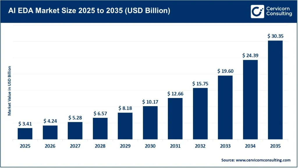
The global AI EDA market was valued at approximately USD 3.41 billion in 2025 and is projected to reach nearly USD 30.35 billion by 2035, expanding at a compound annual growth rate (CAGR) of about 24.5% between 2026 and 2035.
What is the AI EDA Market?
The AI EDA market refers to the segment of the electronic design automation (EDA) industry that integrates artificial intelligence (AI), machine learning (ML), deep learning, and data-driven optimization into semiconductor design workflows. Electronic design automation traditionally includes software platforms used to design, simulate, verify, and validate integrated circuits (ICs), system-on-chips (SoCs), printed circuit boards (PCBs), and semiconductor architectures. With increasing chip complexity driven by advanced computing workloads such as generative AI, autonomous vehicles, high-performance computing (HPC), and 5G infrastructure, AI is now embedded across the semiconductor lifecycle—from front-end architecture exploration to back-end physical layout optimization.
AI-enabled EDA solutions accelerate chip development timelines, improve power-performance-area (PPA) efficiency, automate verification processes, and reduce engineering workloads. These solutions leverage predictive analytics and reinforcement learning to optimize placement, routing, simulation, and verification tasks that were previously manual or rule-based. As semiconductor nodes shrink below 5 nm and chiplet-based architectures become mainstream, AI-native EDA tools are evolving into essential infrastructure for next-generation electronics development.
Why the AI EDA Market is Important?
The AI EDA market plays a critical role in enabling innovation across nearly every modern technology ecosystem. Semiconductor complexity has reached levels where manual workflows cannot keep pace with performance expectations and shrinking time-to-market cycles. AI-driven automation allows chip designers to explore thousands of design alternatives simultaneously and identify optimal architectures with minimal human intervention.
One major reason the AI EDA market is important is its impact on reducing chip design cycles. Traditional semiconductor development cycles can take multiple years, but AI-assisted workflows significantly accelerate simulation, validation, and layout processes. Faster tape-out cycles allow companies to respond quickly to market demands, especially in AI accelerators and edge computing devices.
Another key factor is optimization efficiency. AI algorithms analyze large datasets from previous chip designs to recommend layout strategies that improve power consumption, thermal stability, and transistor density. This capability becomes essential for advanced nodes below 7 nm, where physical constraints become increasingly complex.
The AI EDA market is also strategically important from a geopolitical perspective. Governments worldwide recognize semiconductor design capabilities as critical national infrastructure. Investment in AI-enabled chip design platforms helps countries reduce dependency on foreign supply chains and strengthen domestic semiconductor ecosystems.
Furthermore, AI EDA solutions enable innovation in emerging sectors such as automotive electronics, aerospace systems, healthcare devices, IoT platforms, and quantum computing hardware. Without intelligent design automation platforms, scaling these industries would be significantly slower and more expensive.
Get a Free Sample: https://www.cervicornconsulting.com/sample/2936
AI EDA Market Growth Factors
The AI EDA market is expanding rapidly due to the rising complexity of semiconductor architectures, increasing demand for AI accelerators and custom silicon, growth in cloud-based EDA workflows, adoption of chiplet-based heterogeneous integration, and growing reliance on data-driven verification techniques across automotive and industrial electronics. The transition toward sub-5 nm and advanced process nodes requires predictive optimization tools capable of managing billions of transistors efficiently, while automotive safety standards such as ISO 26262 further increase verification requirements across chip design pipelines.
Additionally, strong investments in semiconductor sovereignty programs across the United States, China, India, Europe, and South Korea are accelerating adoption of domestic EDA ecosystems supported by AI-enabled automation platforms. The proliferation of generative AI workloads is also increasing demand for custom silicon architectures, pushing semiconductor companies toward intelligent automation platforms that reduce tape-out risks and shorten development cycles. Cloud-native EDA platforms are enabling distributed engineering teams to collaborate more efficiently, while the convergence of simulation tools with multiphysics modeling platforms is further enhancing system-level optimization capabilities across next-generation semiconductor ecosystems.
Leading Companies in the AI EDA Market
The AI EDA market is highly consolidated, with a few dominant vendors controlling the majority of global market share. Three companies—Synopsys, Cadence Design Systems, and Siemens Digital Industries Software—collectively account for roughly 75% of the global EDA market.
Below is a structured comparison of key industry participants.
| Company | Specialization | Key Focus Areas | Notable Features | 2024 Revenue | Market Share | Global Presence |
|---|---|---|---|---|---|---|
| Synopsys, Inc. | Semiconductor design automation software & IP solutions | AI-driven chip design, digital verification, silicon lifecycle optimization | Fusion Compiler platform, AI-driven optimization tools, strong IP licensing ecosystem | ~$6B+ | ~31% | Strong presence across North America, Europe, India, China |
| Cadence Design Systems, Inc. | IC design software, verification platforms, system analysis | AI-accelerated simulation, chiplet architecture design, HPC-based verification | Palladium emulation systems, Millennium AI supercomputer platform | ~$4.6B | ~30% | Global operations across semiconductor hubs worldwide |
| Siemens Digital Industries Software | System-level simulation and PCB design tools | Automotive electronics verification, digital twin modeling, heterogeneous integration | Xcelerator platform ecosystem integration | ~Part of Siemens Digital Industries portfolio | ~13% | Europe, U.S., Asia-Pacific |
| Keysight Technologies | Electronic test automation and RF simulation platforms | 5G validation, semiconductor testing, signal integrity analysis | Integrated measurement-EDA workflows | ~$5B+ segment-level electronics solutions | Niche share | Global telecom & aerospace sectors |
| Ansys, Inc. | Multiphysics simulation for semiconductor reliability | Thermal modeling, signal integrity, 3D IC reliability | Advanced system-level simulation engines | ~$2B+ | Simulation-focused niche | Aerospace, automotive, electronics industries |
Cadence alone held roughly 32% share in semiconductor EDA software revenue in 2024, followed by Synopsys at approximately 28%, while Siemens EDA maintained around 18% share.
Leading Trends in the AI EDA Market and Their Impact
1. AI-Native Chip Design Platforms
EDA tools are evolving from rule-based automation systems into AI-native design platforms capable of predicting optimal chip architectures. These platforms leverage reinforcement learning algorithms to improve placement, routing, and verification accuracy.
Impact: Reduces tape-out failures and accelerates development cycles.
2. Cloud-Based EDA Workflows
Cloud-native deployment models allow semiconductor companies to scale compute-intensive simulations on demand. Engineers can run parallel verification workloads across distributed environments.
Impact: Improves collaboration across global engineering teams and reduces infrastructure costs.
3. Chiplet-Based Architecture Design
Modern processors increasingly rely on chiplet architectures rather than monolithic dies. AI-enabled EDA tools optimize interconnect placement across heterogeneous modules.
Impact: Enables scalable semiconductor manufacturing and improves yield efficiency.
4. Integration with Multiphysics Simulation Platforms
The integration of EDA workflows with simulation platforms allows designers to evaluate electrical, thermal, and mechanical performance simultaneously.
Impact: Enhances system-level reliability across automotive, aerospace, and defense applications.
5. Generative AI-Driven Circuit Optimization
Generative AI models are now capable of proposing circuit layouts and architectural configurations automatically.
Impact: Enables design exploration at unprecedented scale.
Successful Examples of AI EDA Market Applications Around the World
Several real-world implementations demonstrate how AI EDA platforms are transforming semiconductor innovation globally.
One notable example is hyperscale cloud providers designing custom AI accelerators using AI-driven layout optimization platforms. These accelerators power large-language-model training infrastructure across data centers worldwide.
Another example is automotive semiconductor companies deploying AI-assisted verification tools to ensure compliance with functional safety standards required for autonomous driving systems. These tools dramatically reduce verification complexity and improve safety validation accuracy.
In the telecommunications sector, 5G chipset developers use AI-enabled RF simulation platforms to optimize signal integrity across high-frequency architectures.
Meanwhile, aerospace manufacturers rely on multiphysics simulation-integrated EDA tools to evaluate thermal performance in mission-critical semiconductor components used in satellites and avionics systems.
Global Regional Analysis Including Government Initiatives and Policies Shaping the Market
North America
North America remains the global leader in AI EDA innovation due to strong semiconductor R&D investments and advanced cloud infrastructure capabilities. The region hosts major EDA vendors such as Synopsys and Cadence, as well as leading chip designers including NVIDIA and AMD.
Government initiatives such as the U.S. CHIPS and Science Act are strengthening domestic semiconductor design capabilities through subsidies and research funding programs. Export-control frameworks also influence global EDA tool distribution strategies.
North America accounted for nearly 29.8% share of the EDA tools market in 2024, reflecting strong technological leadership despite rising competition from Asia.
Asia-Pacific
Asia-Pacific represents the fastest-growing regional market due to strong semiconductor manufacturing ecosystems across Taiwan, South Korea, China, and India.
The region accounted for approximately 42.4% of global EDA market share in 2024, supported by dense semiconductor foundry clusters and increasing government support for domestic chip-design ecosystems.
China is investing heavily in sovereign EDA toolchains to reduce reliance on foreign software platforms, while India is expanding semiconductor design service exports through engineering talent development programs.
South Korea and Taiwan continue strengthening partnerships between foundries and EDA vendors to support next-generation node development.
Europe
Europe plays a strategic role in automotive semiconductor innovation and industrial electronics manufacturing.
Government initiatives such as the European Chips Act are supporting semiconductor sovereignty programs and strengthening local chip design ecosystems. Siemens Digital Industries Software provides strong regional leadership through system-level verification tools integrated with digital twin platforms.
European investments in automotive electronics and industrial automation are increasing adoption of AI-enabled verification tools.
China
China continues investing aggressively in domestic EDA platforms as part of its semiconductor self-reliance strategy.
Government subsidies support local development of placement-and-route engines, SPICE simulators, and verification workflows aimed at replacing imported software technologies. Export-control restrictions from Western countries are accelerating China’s efforts to build independent AI-enabled EDA ecosystems.
India
India is emerging as a strategic semiconductor design services hub supported by its large engineering workforce and increasing participation in global chip-design projects.
Design-service firms in India recorded approximately 17% growth in 2024 as international semiconductor companies outsourced RTL and verification workloads to the region.
Government initiatives such as the India Semiconductor Mission are expected to further accelerate adoption of AI-enabled EDA platforms across domestic chip design startups and research institutions.
To Get Detailed Overview, Contact Us: https://www.cervicornconsulting.com/contact-us
Read Report: Earth Observation Satellite Market Revenue, Trends, and Strategic Insights by 2035